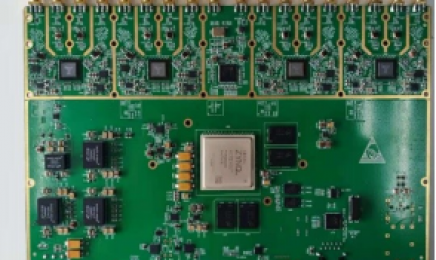
Eight-channel Embedded Software Radio Board With ADRV9009 Chip and Zynq7100 Chip
- The eight-channel embedded software radio platform is an embedded, miniaturized, multi-channel software radio platform developed for vari……
Product Details
The eight-channel embedded software radio platform is an embedded, miniaturized, multi-channel software radio platform developed for various wireless communication product development and communication teaching. The platform is composed of two parts, one is a wireless radio frequency signal transceiver module developed based on ADI 's ADRV9009 chip, and the other is a back-end digital processing module based on Xilinx's Zynq7100 chip. This platform is a high-performance, highly integrated wireless radio frequency signal transceiver processing equipment, suitable for the development of wireless communication teaching aids, miniaturized spectrum
Detection, broadband signal generator, wireless point finding and positioning development, etc. The basic performance indicators of the platform are as follows:
- Baseband processor: ZYNQ7100 integrated dual ARM Cortex™-A9 processors
- Interface: network port, optical port, serial port, USB , TF card, PL port I/O port, JTAG
- Onboard PS DDR3 1GB , PL DDR3 1GB
- Onboard 64MB QSPI FLASH
- SD card slot: can run linux operating system
- Flash and SD card switching: start from flash or from sd card start
- RF channel: 8 send 8 receive
- Sending power: maximum 0dBm
- RF working range: 75MHZ to 6GHZ
- Bandwidth: 200MHz
- Sampling rate: up to 245.76MSPS
- Volume: 23mm (length) × 15mm (width) × 15mm (height)
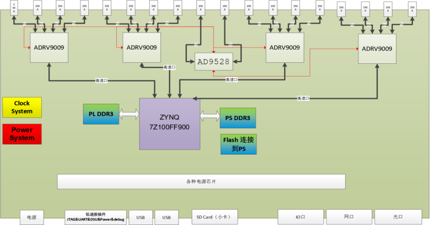
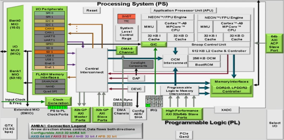
1.1 XC7Z100-2FFG900I
The board uses the Zynq7000 series chip of Xilinx Company, the model is
XC7Z100-2FFG900I. The chip's PS system integrates two ARM Cortex™-A9 processors, AMBA® interconnect, internal memory, external memory interface and peripherals. These peripherals mainly include USB bus interface, Ethernet interface, SD/SDIO interface, I2C bus interface, CAN bus interface, UART interface, GPIO and so on. PS can run independently and start on power-up or reset.
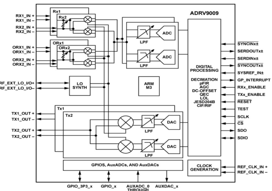
1.2 ADRV9009 chip introduction
ADRV9009 is a high-performance, highly-integrated radio frequency for 5G base station and radar applications
(RF)Agile Transceiver ™ Agile Transceiver . The programmability and wideband capabilities of this device make it ideal for a variety of transceiver applications. The device combines an RF front-end with a flexible mixed-signal baseband section, an integrated frequency synthesizer, and a configurable digital interface to the processor to simplify design-in.
- Has dual receivers;
- Dual input shared observation receiver;
- Maximum receiver bandwidth: 200 MHz ;
- Maximum tunable transmitter synthesis bandwidth: 450 MHz ;
- Maximum observation receiver bandwidth: 450 MHz ;
- JESD204B datapath interface;
- Tuning range: 75 MHz to 6000 MHz
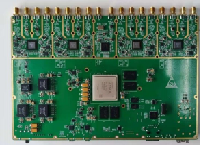
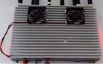
1.3 Board Picture
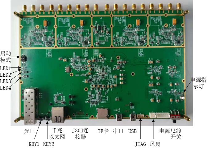
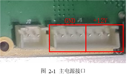
2.1 main power interface
The main power supply adopts +12V power supply, the maximum allowable input voltage is 14V , and the theoretical peak power consumption of the board can reach 80W . It is recommended to use a 12V10A power supply for power supply. The main power interface type is 6 -pin XH2.54 interface.
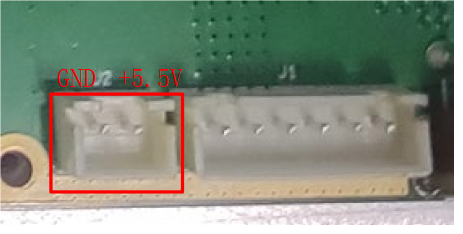
2.2 Fan interface
The board outputs is 5.5V power supply, which can supply power for the fan. When the board is used, please install a fan for good dissipation hot, otherwise there is a risk of burnout.
2.3 clock
2.3.1 PL clock
Onboard The 200MHz clock chip provides the clock for the PL terminal , the clock signal is a differential clock, and the level is standard LVDS .